| Graphensic AB |

| Registration Date | 5 Aug 2018 |
| Revision Date | 5 Aug 2018 |
| Share |
Others Other products
Electronic WaferGraphene
C Graphene CAS Number : 7782-42-5
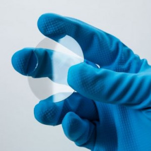
Contact us for inquires regarding 4″ graphene on silicon carbide wafers (SI or N-type), non-standard size samples, bi/few/multi-layer graphene, graphene on off-axis substrates, graphene on 6H or 3C silicon carbide, hydrogen intercalated graphene, and graphene on C-face.
Combining the competence of graphene fabrication with that of processing (Chalmers, Sweden) and quantum metrology (NPL, UK) has empowered, for the first time, the demonstration of a Quantum Hall resistance quantisation accuracy of three parts per billion in monolayer epitaxial graphene at 300mK, four orders of magnitude better than previously reported (Nature Nanotechn., 2010). In 2010, Professors Sirs Konstantin Novoselov and Andre Geim were awarded the Nobel Prize in Physics for isolating the 2D crystal graphene and demonstrating its non-classical physical properties. The same year one of the first EU projects on graphene, ConceptGraphene, aiming at wafer scale electronics, was funded, in which Yakimova supplied the graphene required. In the following years, graphene research has reached unbelievable hype. Yakimova has been involved in graphene-related projects funded by the EUROGRAPHENE programme, FP7 and EMRP Grant Researcher. She is a principal investigator (PI) in work package materials in the Graphene Flagship and a grant holder or PI of several national grants. The area of the graphene on SiC can be as large as that of the substrate. SiC wafers six inches in size are available on the market today and eight-inch wafers are under development. Most importantly, graphene continuity is not broken up by grain boundaries or other extended defects. Specific features of this type of graphene are the step edges which are intrinsically formed due to step bunching in SiC hexagonal polytypes (6H and 4H). An undesirable consequence of this phenomenon is the enhanced Si sublimation at the step edges which facilitates local bilayer graphene formation. The presence of bilayers can affect the sheet resistance of graphene and deteriorate device performance. This is more pronounced and therefore crucial when growing graphene on a wafer scale. The team led by Yakimova has reached sufficient understanding of the operation conditions through comprehensive analysis of the step bunching process and its control during high temperature graphene growth on SiC (Carbon, 2013).