| Silex Microsystems AB |

| Registration Date | 13 Aug 2018 |
| Revision Date | 13 Aug 2018 |
| Share |
Electronics Sensor
Biosensor
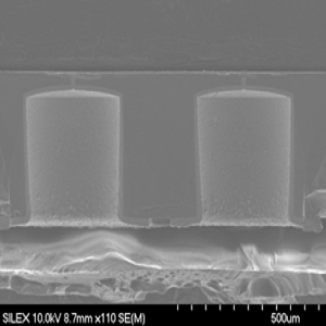
Silex Microsystems, the world’s largest pure-play MEMS foundry, today announced that its Met-Via® full wafer thickness Through Silicon Via is being used to create cost-effective molded chip-level packaging with TMVs. The program, “Chip Architectures by Joint Associated Labs for European Diagnostics,” or CAJAL4EU, is developing nanoelectronics-based biosensor technology platforms enabling in-vitro diagnostic test manufacturers to rapidly build a variety of new multi-parameter test applications in a robust, user-friendly and cost-effective way. Silex’s contributions in this effort include high performance metal through-silicon vias, which will enable through-mold vias for backside signal connections of the CMOS biosensor chip.
“Combining Silex’s Met-Via® interposer with low-cost mold packaging techniques is a big advantage,” says Dr Thorbjörn Ebefors, Chief Technologist at Silex Microsystems. “A silicon interposer with metal TSVs achieves five to 10 times the via density than can be achieved with conventional PCB techniques, resulting in tighter integration and smaller overall solution. Combining epoxy molding techniques from the IC packaging industry and TSV techniques from the MEMS industry, we create a unique and low cost way of routing signals from any CMOS IC to the backside of the package. This not only benefits the CAJAL4EU program, but has wide applicability for ICs in general.”
CAJAL4EU will develop a generalized platform for low cost biofluidic sensing. Biosensing allows for rapid detection of unique biological markers (proteins, antibodies, and other biomarkers for infectious diseases) from microliter fluid samples in an extremely controlled environment. The biosensors will consist of a nanoelectronics-based transducer with an interface chemistry, which makes the connection to the clinical sample to be analyzed. With on-chip detection electronics, small electrical changes can be detected within milliseconds, enabling massively parallel real-time monitoring of bio-molecule binding events. Besides the transducers, interface chemistry and spotting technologies, microfluidics, software and hardware developments (and their integration) will play a crucial role to realize fully integrated biosensor systems and lab-on-chip devices. Therefore, the main deliverables of this project are the different developed technologies: sensor technology including bio-chemical functionalization, microfluidics and related hardware and software drivers.
The complete solution, shown below, includes the CMOS biosensor, the Silex Met-Via interposers, front side redistribution layer (RDL) for connection of the chip to the interposers, and backside RDL for fan-out wafer level chip-scale packaging (WLCSP). The resulting packaging can then be directly mounted onto the system level PCB