
| Analog Devices, Inc. |
Electronics Integrated Circuits Product Number : AD5317R
Integrated Circuits (ICs)Total unadjusted error: ±0.1% of FSR maximum Offset error: ±1.5 mV maximum Gain error: ±0.1% of FSR maximum
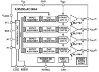
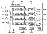
The AD5317R, a member of the nanoDAC® family, is a low power, quad, 10-bit buffered voltage output DAC. The device includes a 2.5 V, 2 ppm/°C internal reference (enabled by default) and a gain select pin giving a full-scale output of 2.5 V (gain = 1) or 5 V (gain = 2). The device operates from a single 2.7 V to 5.5 V supply, is guaranteed monotonic by design, and exhibits less than 0.1% FSR gain error and 1.5 mV offset error performance. The device is available in a 3 mm × 3 mm LFCSP and a TSSOP package. The AD5317R also incorporates a power-on reset circuit and a RSTSEL pin that ensures that the DAC outputs power up to zero scale or midscale and remain at that level until a valid write takes place. Each part contains a per-channel power-down feature that reduces the current consumption of the device to 4 µA at 3 V while in power-down mode. The AD5317R employs a versatile SPI interface that operates at clock rates up to 50 MHz and contains a V LOGIC pin intended for 1.8 V/3 V/5 V logic.
ELECTRONICS - INTEGRATED CIRCUITS

Properties : Offset error: ±1.5 ,Maximum Gain error: ,Total unadjusted er
Application : Data acquisition sys,Digital gain and off,Programmable attenua,Industrial automatio
ELECTRONICS - INTEGRATED CIRCUITS
Properties : Total unadjusted er,Offset error: ±1.5 ,Maximum Gain error:
Application : Industrial automatio,Data acquisition sys,Programmable attenua,Digital gain and off
ELECTRONICS - INTEGRATED CIRCUITS
Properties : Offset error: ±1.5 ,Maximum Gain error: ,Total unadjusted er
Application : Data acquisition sys,Industrial automatio,Digital gain and off,Programmable attenua
ELECTRONICS - INTEGRATED CIRCUITS
Properties : Offset error: ±1.5 ,Maximum Gain error: ,Total unadjusted er
Application : Digital gain and off,Programmable attenua,Industrial automatio,Data acquisition sys


